


Project Overview
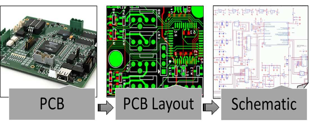
In competitive automobile manufacturing, managing production costs and optimizing spatial efficiency are vital to keeping hardware viable. This project focused on the Reverse Engineering and Redesign of a Production-Grade Printed Circuit Board (PCB).
Using a physical sample, its mechanical enclosure, and baseline legacy design files as engineering references, the project aimed to map out the existing circuit architecture and deliver a modernized, high-efficiency, cost-optimized PCB design. The primary objectives were to minimize the bill of materials (BOM) cost through component localization, optimize the board form factor, and simplify interconnect complexity—all while preserving critical high-power system architectures.
The Challenges
The redesigned PCB had to fit perfectly within the existing enclosure and vehicle assembly without interfering with the upstream wire harness. Several critical challenges shaped the project approach.
The legacy design featured complex connectors with multiple unused I/O pins and oversized connector interfaces, which added unnecessary manufacturing costs and complicated the wiring layout. Additionally, the original PCB relied heavily on imported, expensive, or hard-to-source components, driving up production costs and exposing the client to lead-time bottlenecks and supply chain disruptions.
While the rest of the board was open to redesign and optimization, the primary power sub-circuits—specifically the existing 48V to 12V DC-DC converter layout and the heavy-duty 48V fuse (60A) protection line—had to remain completely unchanged. This required isolating and protecting these high-power areas during the redesign process.
The engineering team had to work within strict project constraints. The scope explicitly excluded comprehensive component stress testing, life-cycle simulations, thermal modelling, and regulatory certifications (e.g., CE, FCC). This meant the redesign had to be structurally sound and layout-accurate right from the start, relying purely on precise spatial assessments and foundational engineering rules.
The redesign had to be structurally sound and layout-accurate right from the start, relying purely on precise spatial assessments and foundational engineering rules.
Solution Implemented by MNES
A structured, data-driven hardware engineering workflow was executed to transition the legacy hardware into an optimized, production-ready design.
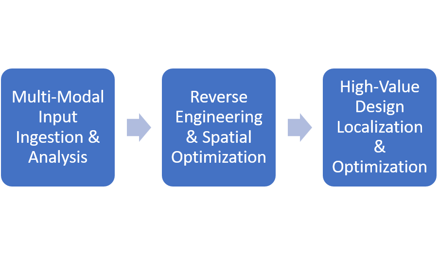
Multi-Modal Input Ingestion
The engineering team gathered and cross-referenced multiple inputs, requiring no further information or clarifications from the client. Physical references included a physical sample PCB board and its mating enclosure box to serve as the definitive baseline for spatial layout. Digital datasets included legacy Gerber fabrication files, schematic drawings, clear board photographs, and a comprehensive eQuad Pin List Excel file.
Reverse Engineering & Spatial Optimization
Form factor evaluation involved analyzing the enclosure and wire harness photographs to determine if the PCB dimensions could be compressed, ensuring any size reductions would not damage or strain the harness. Interconnect simplification involved auditing the eQuad Pin List to identify and eliminate unused pins, replacing expensive legacy connectors with streamlined, cost-effective alternatives that reduced system complexity.
This transformed the design philosophy from:
High-Value Design Localization
The component substitution strategy involved systematically replacing legacy components with technically equivalent, locally available parts. This directly lowered the cost of the PCB and minimized future sourcing risks. The 48V to 12V DC-DC buck circuitry and the 60A safety fuse layout were locked down and accurately transferred to the new layout, ensuring the system's core power distribution remained stable. To maintain branding and continuity, the team prepared to retain the premium black glossy solder mask used on the original board.
Key Results & Deliverables
The project concluded with the successful delivery of an optimized, production-ready engineering package.
Deliverables
- Design Review Report validating all component swaps, spatial changes, and connector optimization strategies
- Revised PCB Layout & Schematic Drawings with modernized, production-grade schematics and trace layouts
- Updated Gerber Files formatted for immediate production with black glossy finish
- Optimized Bill of Materials (BOM) drastically reducing unit manufacturing costs
- Zero-Delay Execution without requiring additional client input
Engineering Impact & Optimization Results
Reduced connector pin count by approximately 30%
Achieved estimated BOM cost reduction of 18–25%
Reduced PCB footprint while maintaining enclosure compatibility
Improved local component sourcing availability and reduced dependency on imported parts
Simplified interconnect architecture for easier manufacturing and maintenance
Key Learnings
- PCB redesign requires balancing electrical performance with enclosure and harness constraints.
- Connector and interconnect optimization helps reduce manufacturing complexity and cost.
- Component localization improves supply chain flexibility and reduces BOM cost.
- Critical high-power circuits must be preserved to maintain system reliability and safety.
- Accurate layout planning is essential when advanced validation and simulation activities are limited.
- Structured reverse engineering workflows improve redesign efficiency and reduce project risk.
Conclusion
The project successfully transformed a legacy automotive PCB into a cost-optimized, production-ready design through reverse engineering, connector rationalization, and component localization.
By preserving critical power architecture while improving manufacturability and sourcing flexibility, the redesign reduced engineering risk and improved long-term production sustainability.